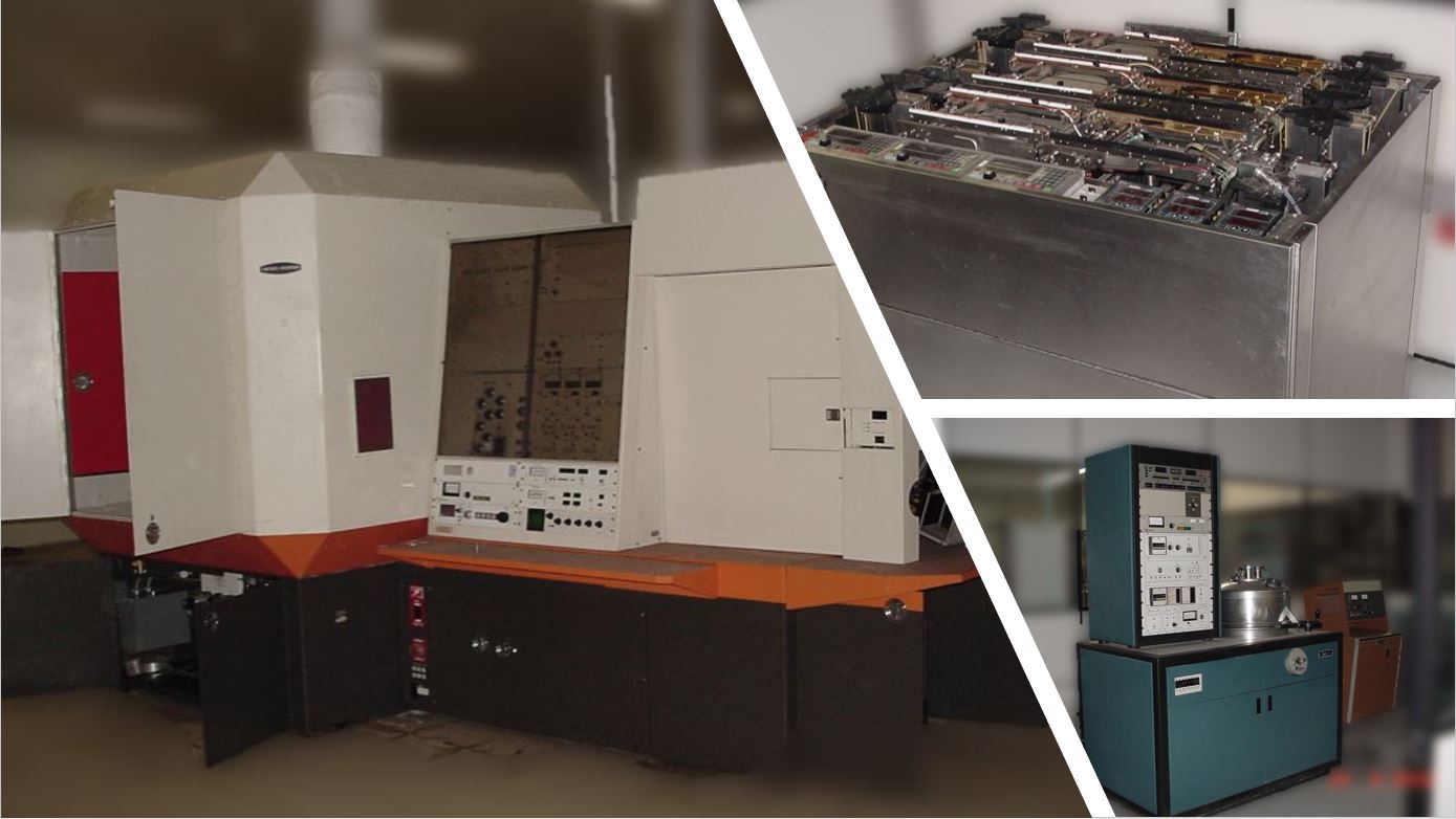
The second, but not less important semiconductor process step, is the wafer doping. The purpose here is to explore the techniques used to growth/deposit films on the wafer surface as a drive-in diffusion pre-step, i.e., the films used as a dopants source with the objective of modify the physical, chemical, or electronic properties of the substrate.
There are different tools available to execute that process. But all of them search for an ideal condition, where the material lost is as small as possible, and the deposited film uniformity, over the wafer surface, is as good as possible in terms of concentration, uniformity and reproducibility.
As per the diffusion type we are intending to use; the doping process will be different.
That´s the reason, I will talk a little bit about the diffusion process. In this post the diffusion will be one of the pre-definitions made to choose the wafer doping process.
As the diffusion mechanism (drive-in) is extremally important, it will be better explored in a future post.
As it´s well known, the diffusion process is associated with the mass transport that occurs in one system, when exists in this system a chemical concentration gradient. Inside the solids, based on the solid type (metal, ceramic, polymer) the diffusion occurs by atomic displacement, by cations or anions, or by macromolecules. It´s dependent on the substrate and the material to be diffused.
For semiconductor, the main mechanism is the atomic displacement, so all the discussion bellow will be based on it.
In a simple way, it can be said that: the diffusion process is dependent on the atoms size (substrate and new material introduced), concentration, time, temperature, and distance from the surface.
From a practical point of view, the diffusion process choice is based on cost, on the impurity surface concentration, on the device’s characteristics, on the junction depth, and in the surface doped area – partial or entire wafer diffusion.
The techniques of doping are based in all pre-definitions for the diffusion process mentioned above, which leads us to three different dopants: solid, gaseous, and liquid.
The techniques most used for wafer doping are spin coating, CVD (chemical vapor deposition) and diffusion from the gas phase deposition.
Spin Coating
The Spin Coating is a process that gives a great film uniformity, allows to work with an extremely high speeds which is helpful to faster drying wafer, and is a very low-cost way to batch process individual substrates. Can be divided in 4 steps: deposition, spin up, spin off and evaporation.
In the Spin Coating process, the wafer is held to a chuck with a vacuum pump, the lid is placed over the spinning basin before the spin is initiated. The spread of the liquid across the wafer is made by a centripetal force.
There are a few process adjustments which could interfere in the film uniformity, such as acceleration, liquid volume, fluid deposition place, particles on the surface prior to spin presence, choice of the dopant, for example, based in volatility, viscosity … all of them influencing completely the final film quality, and therefore the surface doping concentration and diffusion uniformity.
CVD – Chemical Vapor Deposition
The CVD technique to growth film as source for drive-in diffusion process is a technique in which precursors gases react to form film deposits on a substrate. In this process in an atmosphere pressure with flow rates in the laminar regime, source gases are supplied through a gas management system to the inlet of a heated quartz tube by forced and free convection.
The CVD technique is used to produce very pure high-performance solid materials. There are different types of CVD deposition process, based in the activation sources for the chemical reactions such as: thermally activated, laser-assisted or plasma-assisted CVD.
The thermally activated process has the advantage that there is no need for high vacuum (carried out at high pressures). All CVD techniques have the advantages to be deposited on substrates with irregular surfaces and allow deposit on large quantities of closely placed substrates.
The main CVD process parameters, such as temperature, pressure, reactant gas concentration, and total gas flow require accurate control and monitoring.
Diffusion from the gas phase deposition
The diffusion from the gas phase is a technique where a carrier gas is enriched with the desired dopant (also in gaseous form, such as PH3 or B2H6) and transported to the wafers, on which the concentration balance can take place.
This technique is realized inside the same environment where the drive-in process will take place. The diffusion will occur in both wafer sides at the same time, unless you have a layer of SiO2 to prevent it.
The disadvantage here is the fact, where there is not SiO2 as protection, will need to remove the diffusion in one wafer side by lapping, which will cost add to the process.
