I understand that to improve a device characteristic we must know all the manufacturing processes. This is the way we can observe the influence between each process step and its results.
As an example, I chose to use a simple power semiconductor device process, that has the same concepts for other semiconductor devices.
The idea here is to give an overview of all the process steps, the details will be presented in future posts. This overview will be a reference guide to the process sequence that will be explored.
Some of the processes occurs simultaneously, during a production line. I will divide it in front end and back end processes, to get a better comprehension.
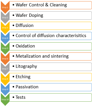
FRONT END Processes – Wafer Processes
This phase will start immediately after the conclusion of the project, where the manufacturing starts.
Imagine we have received the wafers from our supplier….
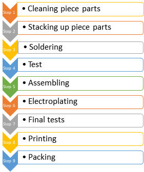
BACK END Processes – Packaging