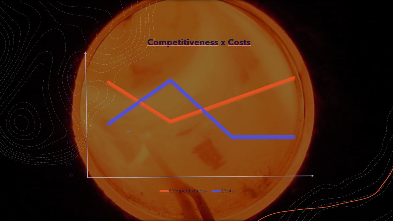
For a semiconductor industry there are a lot of costs that should be well reviewed before implementing any project.
Imagine the following situation, there is a huge addressable market for your product, there are competitors, and you need to beat them to be profitable. What can you offer to make that happen? That´s a question we always ask ourselves to keep us in the market.
Any industry is composed of many interconnected sectors. The product´s cost is calculated based on fixed and variable expenses. For example, in a semiconductor fab, there are infrastructure costs like electrical energy, DI water, compressed air, air-conditioning, clean room, and material costs like substrate, gases, chemicals, headers, etc. and equipment costs, labor, and of course manufacturing processes and others. I will focus on processes.
Did you know the processes in a semiconductor industry represents in average 64% of the total product´s costs?
64% is a lot, don´t you think ? That´s why “Process” has the need to be seen with big eyes.
I will tell you a history that happened to me. It could be taken as a great example of the importance of the process costs …
I visited a fab that produces flexible semiconductor devices and they were facing difficulties with reproducibility, costs and processes. Of course, the three problems were linked. So, I looked for potential issues which they could be facing in their production line. I found a few, but some of them caught my attention.
One of the problems was the choice of material used as ohmic contact and its reasons. I will tell you how I was able to reach that conclusion through a simple question I was asked about.
The question was: Why use aluminum instead of gold in their production? You can have many reasons for that, although gold is still the best metal for ohmic contact, not only for its characteristics but also for its simplicity to work with. But, in that case, the answer was based solely on gold cost, because they believed using aluminum would result in a lower cost. What they weren´t aware of was that it’s not so simple. Due to the high aluminum reactivity, undesired phases are formed, and additional steps should be introduced in the process to eliminate them. They should have predicted and assessed the costs of those additional steps and compared them with the thin gold layer cost before any decision. In their case, the gold layer needed would be very thin, so there would be no undesired phases and no additional steps. As a result, there would be significant improvements in their reproducibility, yield and process.
Even in a case where you will develop new processes or products, old problems and difficulties should be well known and considered to avoid simple fails, capable of compromise your R&D.
Once you define your project, your process choice and its steps will be fundamental to define not only your raw material but also all the resources needed, including your fab structure, and the machinery for your production line. Based in your definitions, a bad choice can easily make you spend a lot more money in machinery for a specific material, turning your cost into a problem.
If you know all your processes from front-end to back-end you will be able to identify your costs bottleneck. That knowledge will enable you to decide where you need to improve or modify your process to bring your costs down.
I think it´s not necessary to say that you can´t compromise your quality to lower your price. But it´s always possible to reduce your cost by improving or creating new processes. Process is a key factor to reach cost reduction.
Process is a place where it´s possible to be creative. There is no rule that dictates specifically which steps must be used or the way you must execute them. What matters is to reach your goal by respecting the quality and specifications.
For example, for power semiconductor devices, the bevel angle (responsible for the reverse voltage) is done mostly by sand blasting each chip, one by one. But it´s possible to bevel hundreds of chips in one wafer simultaneously. We already done that in the production line and the quality was improved and obtained higher yields.
By identifying your process step´s needs, it´s possible to create new solutions, which could impact directly your costs, without losing your device characteristics. In the above example, the beveled angle value and the surface roughness were the two main points to define how far we can go.
The same principle can be applied for digital semiconductors. For example, to deposit the solder alloy elements for the bumping process it´s possible to explore electroplating or even PVD processes. The costs for each one are quite different, but the two of them are feasible.
Based on the film function, you will be able to choose which is the process used to produce that film, the equipment cost, as well as other factors that may increase costs due to adverse effects of that material.
Now, I think one of the best answers for the initial question of this post, is to work with your processes to reduce your costs and keep you in the market, Don´t you agree?
