Hi! Today I invite you to participate of this post, because I will compare different semiconductor technologies based in their characteristics and manufacturing processes.
I think a good starting point is to divide the semiconductor in this post in two groups: power semiconductors devices and digital or mixed-signal devices.
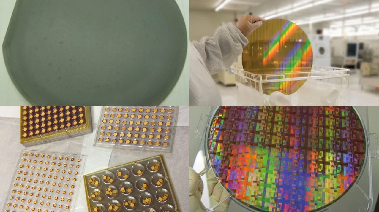
In the first group I will discuss power semiconductor devices. In this area there are two technologies: planar and bipolar. For both of them its work with: large semiconductor areas (mm2 or cm2) uniformities, high doping concentrations (1020 atoms/cm-3), thin and thick films, high currents and voltages, big packs, large contact areas, high torque, a lot of mechanicals efforts, high values of heat dissipation, huge thermal expansion coefficient between different materials …
For the second group, I will discuss digital or mixed signal technologies. In this area they have low voltage and low current devices with: small areas (micro or nano technologies) uniformities, lower dopants levels (1017 atoms/cm-3), mostly thin films, small packs, most packs are soldered in a board, you don´t have mechanicals efforts for the pack (torque) but you do have stress between the films grown, a lot of thermodynamics ….
In the first group mentioned above the frontend manufacturing processes follows the same logic, but for bipolar technologies there are more steps of photolithography and thin film growth than in the planar. In this case techniques like CVD, PECVD, Sputtering, plasma etch are frequently used.
In power semiconductor devices, for frontend steps are used a lot of thermal processes, such as diffusion, sintering, oxidation, metallization, and sometimes also with soldering (especially for disc types). It can´t be forgotten to mention the electron irradiation, used, to introduce recombination centers in the band gap to reduce the reverse recovery time of the device, turning it into a fast recovery device.
In the backend for power semiconductor devices there is a lot of R&D in the packaging area, where lies the limit of its use. The pack´s choice can interfere in the heat exchange due to the dissipation during the conduction. This is a great reason to have a lot of engineering here.
The backend can be divided in assembling, packing and testing, in all three areas there are large packs with different technologies such as glass-to-metal-seal, ceramics seals, organic seals. The choice of the packing interferes not only in the assembling manufacturing processes but also in the frontend manufacturing processes. The most interesting here is that any of the choices deals with large areas of solder, large thermal expansion coefficient as well with different and complex centralization processes.
Now for the second group mentioned before, the digital or mixed-signals devices, it is used ion implantation, thin films depositions and etching techniques several times. The etching processes of these thin films can be done by dry process or wet solutions. In the dry process there is a lot of techniques used such as PECVD, sputtering, plasma etching, and others.
In this group there are memories and flexible MEMS or even flexible IC. All of them are based on MOS technology. There are the traditional ones where the substrate is electrically active because they are part of the device, and the ones that the substrate is part of the base and don´t interfere with the device electrically once it is an insulator and act only as mechanical support of the flexible IC.
As an example, think on the flexible printed tags, the manufacturing process is based completely in film deposition and corrosion. The substrate, in this case, doesn´t interact electrically with the device, but it´s part of the base of the device. The semiconductor is grown as films over this polymer.
For small devices it´s used different solder technics: like bumping soldering. The metallization process can be in vacuum, electrolytically or electroless. The centralization of the solder for each device is always made by photolithography, which differs from the power semiconductor device presented before.
Besides all those differences presented here, it is important to remember that there are differences in morphology and crystallography of the wafers for each application.
The main idea here, is that even changing semiconductor areas, the semiconductors and the manufacturing process principles are the same for the two groups of devices presented in this post. Of course, based in the dimensional you will have different problems or even difficulties, but most of them have the same theory and could be thought by the same technologies.
For power semiconductors devices, from the point of view of the process, the larger areas, the huge heat dissipation, the mechanics of the assembling is of prime importance.
I think right now it is time to talk about costs… don´t you agree? So, for the next post I will talk about it, always looking from the process perspective. In this case if you would like to ask me to talk about something, I will be glad to write about it.
