Project, as we know, is a temporary effort undertaken to create a product, service or result. It always has a programmed start and an end.
Projects are typically created based on problem solving needs, or business opportunities.
The starting point of the projects, after their initial definition, is the collection of data to foster the entire technical study. It is important to note that the technical study, in addition to product development, often requires the process study and its integration with the project itself.
The idea of this blog is to have the opportunity to present and discuss semiconductors devices, so I will focus on a device project.
For semiconductors, all the data gathered needs to be transformed into electrical language. That done, we will have the necessary information to calculate and scale the new device.
Once the project of this new device is defined, starts communication with the factory. Here the integration between device project and manufacturing processes would start.
Knowledge of the manufacturing processes and its difficulties is extremely important for the success of the project. There are processes, equipment and material limitations that need to be well studied in order to make any project feasible.
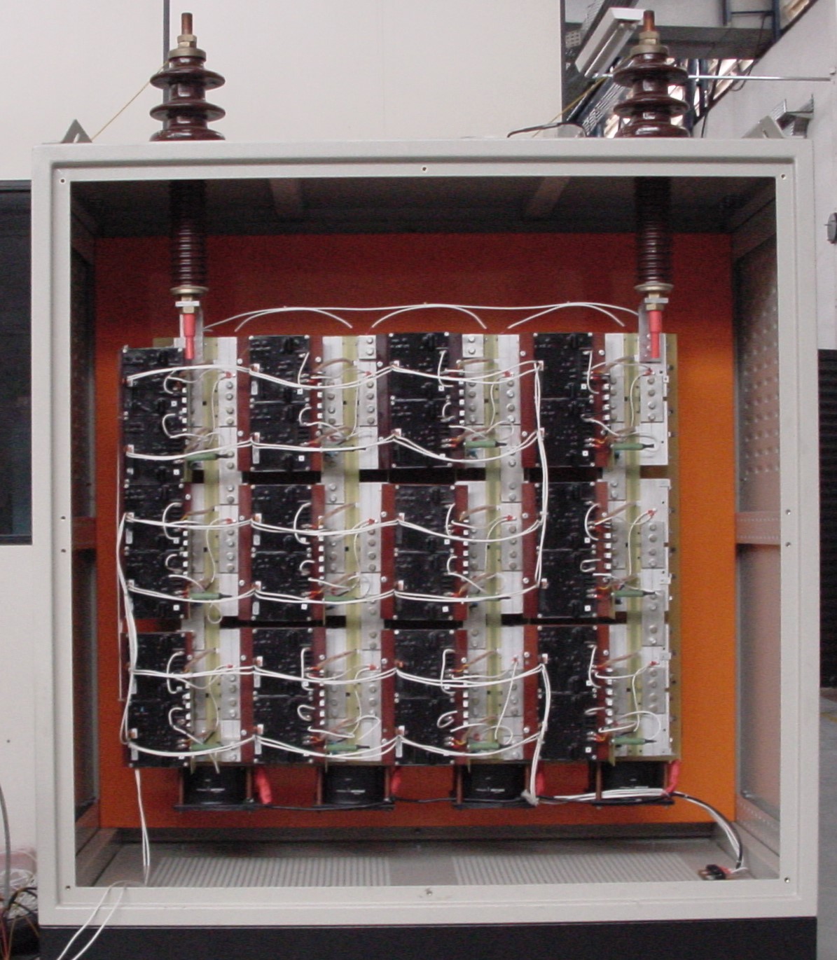
After the feasibility phase, the development will come into effect. In this part we will start to choose the materials involved, manufacturing processes, tests and finally follow-up analysis.
At this point, I would like to call your attention, that I will focus mainly on silicon as a starting material.
The first item to be discussed here is the substrate. The type of substrate to be processed enters this discussion – group III-V, silicon, polymeric or new substrates; in case of silicon the wafer – monocrystalline, polycrystalline or amorphous; the crystallographic orientation for monocrystalline wafers – (111), (100), (110), type n or p and all the specifications of the substrate.
Together with the wafer definition comes the wafer pulling process, for example, for silicon it could be “FZ – Float Zone”, “CZ – Czochralski” or “NTD –Neutron Transmutation Doped”.
Each type of wafer growth influences the electrical results as well as this device cost.
The selection of the wafer is always based on cost-effectiveness.
It is important to emphasize here that the cheapest material is not always the best choice, once the selection of this material may require the addition of new process steps to overpass problems that may come from the characteristics of the chosen material, and for this reason end up making the final product more expensive.
Once the wafer is defined, the substrate to be worked with is defined. The next stage of the process will be based on the electrical characteristics intended, according to its use.
For example, for power semiconductor devices, we normally need to have a highly doped surface, maintaining the surface concentration of the order of 1020 atoms of boron and phosphorus and with gallium the surface concentration a little bit lower. The junctions are deeper, also requiring uniformity of the dopant over the entire wafer. Because junction depth is high, high diffusion temperatures are used on the order of 1250 C°.
In case of low voltage or nanoscale devices junctions are usually created, mainly by the growth of thin films. The areas are constantly demarcated by the use of photolithography, in order to limit the growth of the film as accurately as possible. Many of the diffusion processes here are carried out by ion implantation. The surfaces here are in the order of 1017 doping atoms/cm3.
In addition, we have all the others manufacturing process to continue the development of the new device.
What I would like to show you here is not how to carry out the project, but how the dimensioning of the new product and its process interlace. Both are critical to the success of the new product.
Dimensioning defines the initial points of the project while the process materializes the new product, counting the feasibility or not of this project.
That is why it is very important to keep in mind that a viable project, the correct dimensioning of the device, as well as the chosen processes for the manufacture of this new device, have upmost importance for the success of this project.
